Cortex M4 core, memory map, and Thumb instructions
Cortex M4 features
Section titled “Cortex M4 features”The Cortex M4 is a 32-bit load-store RISC core, with Harvard architecture. It has a three-stage pipeline (fetch, decode, execute) with branch speculation and two sleep modes: wait for interrupt (WFI) and wait for event (WFE).
There’s support for debugging and tracing programs with breakpoints, watchpoints and optional execution trace.
Other features include DSP instructions such as hardware multiplication, MAC, and saturation, plus optionally an FPU.
Block diagram
Section titled “Block diagram”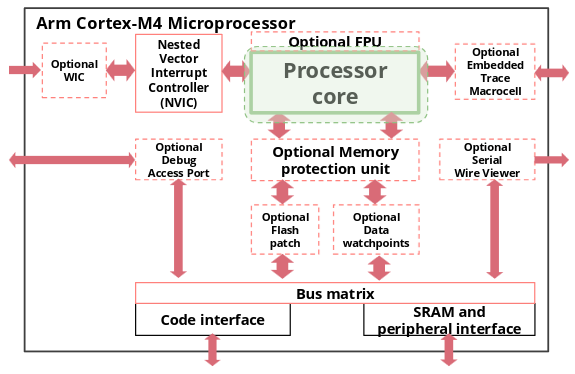
- Processor core
- contains internal registers, the ALU, the data path and some control logic.
- Nested vectored interrupt controller (NVIC)
- automatically handles nested interrupts (for example allows a high priority interrupt to execute even if another low priority one is executing).
- Wake-up interrupt controller (WIC)
- in low power modes, the processor disables most of the system. When an interrupt request is detected, this component powers up the processor.
- Memory protection unit (MPU)
- makes some regions of memory read-only or prevents unprivileged applications from accessing them.
- Embedded trace macrocell
- can record if an instruction was executed or not.
- Data watchpoint
- can observe selected data accesses.
- Serial wire viewer
- streams selected trace data over a low-pin interface.
- Bus matrix
- provides data transfer capabilities among hardware components and peripherals. It allows data transfers to take place on different buses simultaneously.
There are two buses:
- Advanced High-performance Bus (AHB): used for high-bandwidth peripherals;
- Advanced Peripheral Bus (APB): low-power, used for other simpler peripherals;
Programming model
Section titled “Programming model”The set of registers available for use by programs is called the programming model. The CPU has many other registers that are used for internal operations.
The load-store architecture requires that data is loaded from memory into registers and stored from registers to memory using dedicated instructions.
The Cortex M4 features 16 32-bit registers, of which:
- R0 - R12 are general purpose (R8-R12 cannot be used by all instructions).
- R13 is the Stack Pointer (SP) that records the current address of the stack.
- The Program Counter (PC) records the address of the current instruction and is automatically incremented by 4 after each instruction.
- R14 is the Link Register (LR), used to store the return address of a subroutine or function call.
Another special register is the Combined Program Status Register (xPSR), which provides information about program execution and ALU flags. It is the combination of Application PSR (APSR, ALU flags), Interrupt PSR (IPSR) and Execution PSR (EPSR).
Memory map
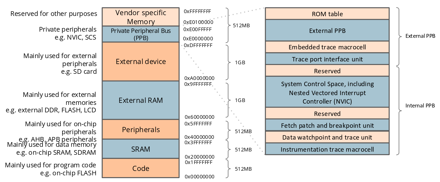
Section titled “Memory map”The memory map describes the organization of the processor’s address space. ARM memory is byte-addressable using 32-bit addresses with a maximum address space of 4 GB.
The memory space is subdivided into a number of regions, each with a particular recommended use.
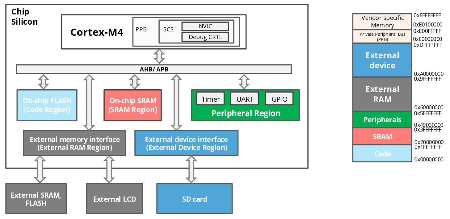
- Code region
- primarily used to store code or data memory.
- SRAM region
- primarily used to store runtime data such as heaps and stacks.
- Peripheral region
- used to access peripherals on the chip’s bus by mapping them to memory addresses.
- External RAM and external device
- used for external memories or peripherals.
- Private peripherals bus
- used for the NVIC and SCS.
Bit-band operations
Section titled “Bit-band operations”Bit-band operations allow a single load/store operation to access a single bit in the memory. Without bit-band we would need to read the 32-bit word at the address into a register, modify the bit, and write back all 32 bits.
Endianness
Section titled “Endianness”Endian refers to the order of bytes stored in memory:
- Little-endian stores the lowest byte of a word in bits 0 to 7.
- Big-endian stores the lowest byte of a word in bits 24 to 31.
The Cortex M4 supports both little and big endian.
Thumb instruction set
Section titled “Thumb instruction set”Early ARM instruction sets had only 32-bit instructions, which were powerful and provided good performance, but they occupied more program memory compared to 8- and 16-bit processors and resulted in a larger power consumption, as more information needed to be moved in and out of memory.
The Thumb-1 instruction set introduces 16-bit instructions (a subset of the ARM instruction set), which allowed reducing code size, but sometimes needed to perform more operations, making code slower. A multiplexer is used to switch between two states, which introduces an additional overhead.
The Thumb-2 instruction set introduced other 32-bit Thumb instructions which allow to reduce code size, but maintain similar performance to ARM.
Most Thumb-2 instructions are unconditional, whereas almost all ARM instructions can be conditional (not only branches and jumps).
Embedded program development
Section titled “Embedded program development”The typical program generation flow consists of compiling code into object files, which the linker turns into one image whose bytes have defined storage and runtime addresses.
The program image will then be stored in the code memory region of the microcontroller.
It typically contains:
- Vector table: with the starting addresses of interrupt routines. The first is the main stack pointer (MSP), then there is the Reset Handler address and then exception and interrupt handlers.
- C start-up code: used to set up data memory and initialize global variables. It is inserted automatically by the compiler/linker.
- Program and library code
After a reset, the processor reads the MSP value, then reads the reset vector value, branches to the start of the reset handler, and starts executing instructions.